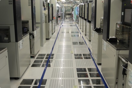
Since 2007, WIN Semiconductors Corp. is the largest 6 inch (150 mm) GaAs pure play foundry in the world. WIN has three advanced fabs with a broad range of technology providing the best quality of HBT, pHEMT, BiHEMT, GaN foundry services for MMIC application. Since 2006, WIN has operated a 4 shift 24/7 non-stop foundry service. Our annual capacity has exceeded 340,000 wafers in 2018 and has become the world biggest GaAs foundries fulfilling more than 50% of the global GaAs foundry demand.
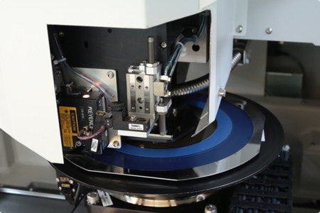
In addition to advanced semiconductor fabrication technology, WIN also provides layout support and automated DC/RF on-wafer testing. WIN is committed to fast turnaround time, cost-effective turn-key solutions and total quality control for our valuable customers.
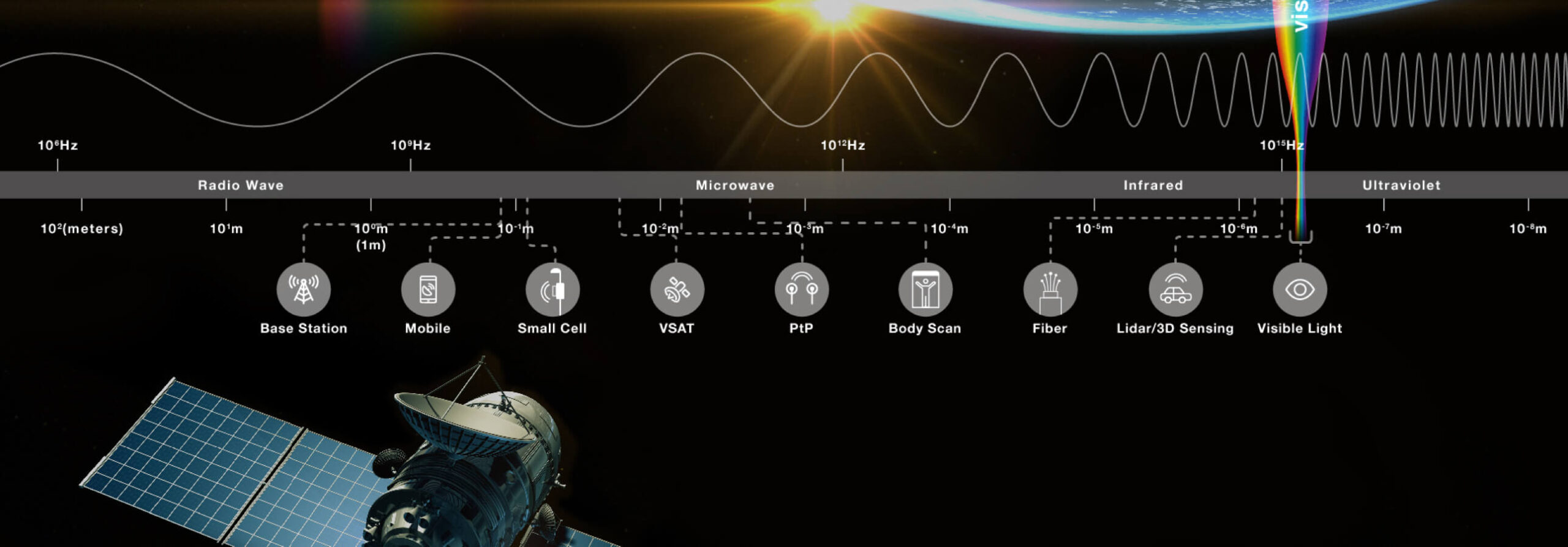
III-V compound semiconductor devices, with their ability to function at higher frequencies, have been the preferred technology to implement wireless application for aerospace service. With the exploding demand in commercial broadband/wireless communication and optical communication, compound semiconductor process technology is now widely applied in high frequency, high power, low noise, and optoelectronic products.
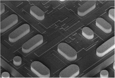
WIN’s technology team has substantial experience in GaAs HBT and HEMT MMIC fabrication. This team is familiar with the latest developments in GaAs technology, and will provide continuous research and development to meet our customers' technology requirements. In addition to MMIC technology, WIN has also established optoelectronic device technology such as compound semiconductor lasers and photodiodes. The service embodies Epi-wafer growth, optoelectronic device fabrication, and device characterization.
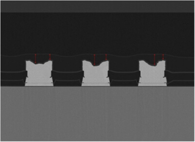
WIN's technology roadmap covers both HBT and HEMT processes. More than 20 processes are available and production-ready. WIN will continue to provide various cutting-edge processes to keep our customers ahead of the game.
In addition, in terms of the breadth of the technology, the primary compound semiconductor materials have expanded from GaAs to GaN in order to satisfy the diverse wireless communication needs. In terms of market application, we have actively focused on the R&D for 5G infrastructure and optical communications technologies under the Internet of Things (IoT) trend in order to capture future market opportunities.
WIN provides various optional processes to fullfill various unique application requirements and package technology. That approach enables highly integrated product design and superior performance with advanced packaging.